Blue View
Project Blue’s free critical materials analysis - commentary, insight and video in one place.
Refine your search
- EVelution Energy enters cobalt offtake agreement with MitsuiNEWS
- The Democratic Republic of the Congo’s audit push reinforces state oversight over cobalt export flowsNEWS
- OFZ’s production launch in Uzbekistan delayed once moreNEWS
- Mineral Resources raises lithium production guidance for Mt Marion and Wodgina NEWS
- MPW joins UK defence supply chain through titanium additive manufacturingNEWS
- How scandium and yttrium shortages are tightening aerospace and semiconductor supply chainsOPINION
- The USA pushes for independence from China for NdFeB magnet supplyOPINION
- Rare earth supply and impacts under China's new quota rulesOPINION
- India’s battery recycling: big opportunity, different playbook? OPINION
- New ferrosilicon plant under construction in BhutanNEWS
- CESCO Copper Week 2026, Santiago: key talking pointsNEWS
- USA Rare Earths announces acquisition of Serra Verde Group in US$2.8Bn dealNEWS
- China’s Hailiang to establish new copper processing JV in Saudi Arabia NEWS
- Changan deploys first sodium-ion-powered electric vehicleOPINION
- Indonesia to incorporate by-product pricing as part of nickel ore benchmark (HPM)NEWS
- US International Development Finance Corporation to invest in antimonyNEWS
- Malaysia Smelting Corporation begins construction of new crude tin smelter NEWS
- Lithium-ion long-duration energy storage begins to enter the mainstream NEWS
- Fireweed Metals expected to raise US$44.3M through private placement backed by strong investmentNEWS
- German Salzgitter launches critical metals recovery research projectNEWS
- Environmental report for HF pilot plant submitted to Tasmanian EPA NEWS
- Ivanhoe Mines cuts 2026–2027 copper production forecastNEWS
- 9% of global aluminium output potentially caught up in the Iran warNEWS
- Syrah Resources announces plans to restructure its balance sheetNEWS
- Record tin production at Andrada’s Uis mineNEWS
- US International Trade Commission rejects combined ~160% tariffs on Chinese active anode material imports NEWS
- Australian fluorspar project receives approval from Japanese partners NEWS
- Indonesia plans export and windfall taxes on nickel and coalNEWS
- Lyten advances its Northvolt takeover and unveils multi-technology battery plans in GermanyNEWS
- Russia to auction niobium deposit in Krasnoyarsk regionNEWS
- Almonty Industries commissions its Sangdong tungsten mine in South KoreaNEWS
- Risks to industrial mineral markets as sulphur shipping disruptions continueNEWS
- Organic fluoride electrolytes: an alternative path for liquid lithium batteriesNEWS
- US uncertainty influences global polysilicon market outlookOPINION
- Volatile tin market raises risks for downstream industryOPINION
- Western germanium supply shortage exacerbated by rising demandOPINION
- The USA moves from dependence to optionality for gallium supplyOPINION
- Centaurus Metals seals nickel offtake deal with Glencore from Jaguar Nickel Sulphide ProjectNEWS
- Australia backs vanadium development as Queensland opens new mining areasNEWS
- End of the road for Viridian LithiumNEWS
- China’s “Two Sessions”: our takeaways and implications for critical industriesOPINION
- BYD unveils new flash charging technology: dual breakthroughs in battery and charging infrastructureNEWS
- Aluminium Bahrain invokes force majeure amid shipping disruptionNEWS
- Sulphur supply chains through Hormuz reveal risks in energy transition materialsOPINION
- QatarEnergy announces aluminium production suspensionNEWS
- Rio Tinto to construct gallium demonstration plant in CanadaNEWS
- Donut Lab releases solid state battery test report: an interpretationNEWS
- Group1 and Michigan Potash & Salt Co sign MoU for Potash-to-Battery supply chainNEWS
- Quantifying critical material flows in the aerospace sectorOPINION
- Zimbabwe bans lithium exports with immediate effectNEWS
- What is the impact of rising lithium costs on LiPF6?OPINION
- China adds 20 Japanese entities to dual-use export control list NEWS
- Solid-state battery anode materials: technological evolution and industrial trendsNEWS
- Largo is ready to increase vanadium supply to the USA as tariffs are struck downNEWS
- Lion smelter restart follows interim electricity tariff approvalNEWS
- Only US fluorspar mine begins productionNEWS
- Shifting Critical Material World Order: EVs and Li-ion Batteries REPORT
- Securing the Transition: What's Changing in Critical Material Supply Chains in 2026REPORT
- Lithium 2040: The element shaping our futureREPORT
- Trade Tensions and Critical MaterialsREPORT
- Consulting Insights: From Challenge to OpportunityREPORT
- South Africa's Evolving Role in Global Ferroalloy MarketsREPORT
- Critical Materials and the Defence SectorREPORT
- China's 15th Five-Year PlanREPORT
- Copper use in data centresNEWS
- ElevenEs raises Series B to advance Serbian LFP plant NEWS
- Metals and the Security of NationsREPORT
- Sherritt pauses Moa operations in Cuba due to fuel shortagesNEWS
- Metal Markets in TransitionREPORT
- Top 5 Calls for 2025REPORT
- Will developments in China drive tungsten prices to new highs in 2026?OPINION
- Weda Bay Nickel receives sharply reduced 2026 quotaNEWS
- Low cost LFP batteries are outcompeting NCM batteriesNEWS
- Rio Tinto–Glencore: until next timeNEWS
- Project Vault and US supply chain resilienceOPINION
- US Defense Logistics Agency seeks long-term vanadium pentoxide supplyNEWS
- USA bolsters downstream germanium refining capabilities for military applications NEWS
- Canada Nickel’s Crawford Project advanced under Ontario’s “One Project, One Process” frameworkNEWS
- Pangang Group and Dalian Rongke forge 2026 supply pact, bolstering the vanadium flow battery ecosystemNEWS
- CATL’s supply deal with Ningbo Ronbay: impact on the LFP CAM marketOPINION
- EV sector to drive growth in European battery demandOPINION
- Indonesia addresses tin market frenzy with benchmark price NEWS
- IperionX strengthens US titanium supply chain with federal funding and US Army contractNEWS
- US government backs USA Rare Earth to build domestic heavy rare earth supply chainsNEWS
- Rio Tinto–Glencore: copper, coal, and culture OPINION
- Which metals are critical to jet engine supply chains?OPINION
- Alphamin Resources achieves record tin production in 2025 NEWS
- US Government supports strategic fluorspar stockpileNEWS
- Mutoshi sale complicated by competing interests and Gécamines’ entryNEWS
- Zijin Mining and JDC partner to build domestic molybdenum capacity in China NEWS
- Mkango, HyProMag and the University of Birmingham open the Tyseley Rare Earth Magnet Recycling plantNEWS
- Magrathea Metals secures offtake and funding with Wogen ResourcesNEWS
- From dependence to optionality: the USA makes another investment in gallium and germanium NEWS
- High copper prices persist in early 2026NEWS
- Which materials are critical to airframe supply chains?OPINION
- Abolition of administratively determined time-of-use pricing ushers in a new era for energy storageNEWS
- Australia strengthens critical minerals strategy with new strategic reserveNEWS
- PT Vale Indonesia halts nickel ore mining amid delay to 2026 RKAB approvalNEWS
- China moves to ban exports of key critical materials to Japanese consumers under tighter dual-use restrictions NEWS
- Egyptian silicon metal project secures additional financingNEWS
- US must ramp up titanium capacity to avoid squeezeOPINION
- VinFast’s Indonesia bet: regional expansion amid mounting financial pressureNEWS
- PT KNI delivers first autoclave at Indonesian HPAL projectNEWS
- Gécamines and Mercuria form joint venture to commercialise the DRC’s Cu-CoNEWS
- Hype fades as the future of vanadium flow batteries grows uncertainNEWS
- Copper demand to grow 35% by 2035, driven by construction, utility networks, renewable energy and EV sectorsNEWS
- Jervois Global to restart its São Miguel Paulista nickel-cobalt refinery in Brazil NEWS
- Dubai Airshow 2025 highlights: market activity, industrial expansion, and sector-wide challenges NEWS
- Extracting value from waste: the USA pursues domestic scandium and gallium productionOPINION
- Tailings constraints at Indonesian HPALs threaten growing nickel and cobalt capacityNEWS
- Key findings from the 2025 China International Lithium Industry ConferenceNEWS
- Australian Vanadium receives additional funds for vanadium project developmentNEWS
- EV sales continue to climb globally with policy a core driverNEWS
- Vanadium outlook for 2026: Will energy storage offset steel’s slowdown?VIDEO
- Safeguard measures approved for EU silicon and manganese alloys OPINION
- Kazakhstan launches giant ferrosilicon plantNEWS
- Simandou’s first shipment: a three-decade epilogue and a turning point for the iron ore industry NEWS
- Molybdenum market shifts: Copper dependency meets geopolitical tensionsVIDEO
- Ferroalloys in focus: 2025 market review and strategic outlook for 2026VIDEO
- The Project Blue Story: Market Intelligence for the Critical Materials EraVIDEO
- The impacts of suspending the ban on Ga–Ge–Sb exports to the USA OPINION
- Japan’s copper smelters move to consolidate amid margin pressureNEWS
- MinRes and POSCO Holdings form new lithium joint ventureNEWS
- American Tungsten to potentially receive support from US EXIMNEWS
- RHI Magnesita reports ten-month results amid challenging demand backdropNEWS
- How Project Blue’s Consulting team delivers strategic insights for critical material supply chainsVIDEO
- End-of-life battery supply expands: the ABTC is awarded the largest lithium-ion clean-up and recycling contract in EPA historyNEWS
- Successful processing trial at Hemerdon MineNEWS
- Ferro-Alloy Resources appoints contractor to begin construction on Kazakhstan vanadium projectNEWS
- Global ferroalloys leaders reflect on key insights from Project Blue’s Critical Materials Conference: Ferroalloys 2025VIDEO
- US investment firm wins bid to develop Kazakhstan tungsten projectsNEWS
- China’s rise to battery recycling dominanceVIDEO
- EV battery demand: growth, policy shifts, and the recycling imperativeVIDEO
- Regulation takes centre stage in battery recyclingVIDEO
- The rise of battery recycling: ESS and EVs in focusVIDEO
- China’s LB Group tightens hold on global TiO2 capacity with UK acquisitionNEWS
- Outokumpu to invest in a new chrome plant in the USANEWS
- China to suspend rare earth export controls for one year NEWS
- Almonty expands its mining portfolio with US tungsten project acquisitionNEWS
- JPMorgan and Agnico Eagle invest in Perpetua Resources’ US antimony projectNEWS
- European Union includes Evraz on sanctions listNEWS
- Constructive conversations at the 2025 Joburg IndabaNEWS
- Will vanadium supply pressure persist over the near term?OPINION
- Molymet expands in the USA with the creation of Molymet AlloysNEWS
- Korea Zinc doubles up on critical materials with gallium recovery circuit in UlsanNEWS
- A fragile truce: how could dual export controls reshape the global aerospace industry?OPINION
- US and Australian governments to support gallium development with AlcoaNEWS
- Turning policy into progress: monitoring critical mineral commitmentsOPINION
- China’s molybdenum export controls place a spotlight on a strategic metal NEWS
- Tin concentrate tightness persists as Man Maw stays shutNEWS
- Indonesia’s shifting RKAB policy and implications for nickel supplyNEWS
- China’s anti-involution crackdown poses risk to lepidolite supplyNEWS
- China’s Q3 GDP growth of 4.8%: a slowing trend but still in line with Beijing’s objectiveNEWS
- Tightening feedstock availability expected to support cobalt pricesNEWS
- Rethinking secondary aluminium flows in light of global structural demand NEWS
- Copper e-scrap trends: from supplementary feed to strategic resource NEWS
- China tightens export controls on battery materials and core equipmentNEWS
- China's Ministry of Commerce announces enhanced export controls on rare earths OPINION
- Teck Resources lowers Quebrada Blanca copper production guidanceNEWS
- Project Blue Shares Insights on Secondary Copper Market at the ICSG MeetingNEWS
- Global Advanced Metals to supply the US Defense Logistics Agency over the next five yearsNEWS
- Chinese fluorspar capacity expands with new Ka’erqia’er mineNEWS
- Agreement reached between US Department of Energy and Lithium Americas regarding loanNEWS
- Alcoa to permanently close its alumina refinery in Western Australia NEWS
- Vale boosts Onça Puma output with second furnace start-upNEWS
- Accelerating US funding for antimony security NEWS
- Updated Preliminary Economic Assessment for the South Crofty project highlights attractive economicsNEWS
- Freeport-McMoRan declares force majeure at Grasberg mineNEWS
- Ferroglobe suspends silicon metal production in Europe NEWS
- Rio Tinto to supply scandium to the US National Defence StockpileNEWS
- Moroccan chemical manufacturer receives US$110M for its fluorine recovery projectNEWS
- Chinese government sets 180GW target for energy storage installations within two yearsNEWS
- Neo Performance Materials opens Narva NdFeB magnet production facilityNEWS
- China responds to US Department of Commerce adding 23 more Chinese companies to its Entity ListNEWS
- DRC to replace cobalt export ban with quotasNEWS
- China’s integrated circuit production reaches a historic highNEWS
- Superior Graphite has entered into a strategic agreement with the energy giant, ExxonMobilNEWS
- Lopal Technology’s journey of expansion behind the agreement with CATLNEWS
- New graphite supply increases Tanzania’s market shareNEWS
- Aurubis signs a €200M loan with the European Investment Bank to finance copper expansionsNEWS
- US Li-ion recycling: recent developments under policy shifts and price swingsNEWS
- Anglo Teck: from takeover targets to market leaders OPINION
- Portion of Weda Bay Nickel site reclaimed over forestry permit issueNEWS
- Mercedes-AMG debuts quadruple-element lithium battery with revolutionary immersion cooling systemNEWS
- Anglo American and Teck Resources announce a merger of equalsOPINION
- CATL holds meeting to accelerate reopening of the Jianxiawo Lithium MineNEWS
- Talison Lithium moves towards environmental greenlight for Greenbushes mine expansionNEWS
- Critical Materials, Critical Missions: Securing Supply Chains for Defence ReadinessOPINION
- ATI bolsters its aerospace titanium position with a new facility and OEM agreementsNEWS
- JS Link America announces construction of NdFeB magnet facility in Georgia, USANEWS
- US and EU germanium prices surge as material remains scarce NEWS
- Glencore’s layoff plans threaten South Africa’s last stable vanadium operationNEWS
- How will copper miners be affected by the DRC's cobalt export ban?OPINION
- St. Lawrence fluorspar mine restartNEWS
- China fluorspar updates: new mines and expansionsNEWS
- Korea Zinc and Lockheed Martin sign MoU for germanium supply and procurementNEWS
- What’s behind the surge in tungsten prices?OPINION
- Setbacks continue to plague lithium-ion battery cell pipelineNEWS
- US government acquires 9.9% stake in IntelNEWS
- What are the ripple effects of the DRC’s cobalt export ban?OPINION
- EU-USA trade agreement follows new tariffs on over 400 aluminium and steel productsNEWS
- Mozal Aluminium to potentially shut down in 2026NEWS
- Fluorspar search at REE project in MozambiqueNEWS
- Kenyan fluorspar processing plant to be refurbishedNEWS
- CATL expands into battery refurbishment business NEWS
- Digging into copper costs: Concentrate vs SX-EW and the road aheadOPINION
- Copper margins: a decade in reviewNEWS
- Lyten acquires remaining Northvolt assets in Sweden and Germany NEWS
- NextSource & Mitsubishi sign an offtake agreement for coated spherical purified graphiteNEWS
- Do the EU’s antidumping tariffs on Chinese fused alumina imports hinder more than help the domestic sector?OPINION
- CATL halts lithium mineral production at Jianxiawo lepidolite mineNEWS
- SAIC launches its first LMO semi-solid-state batteryNEWS
- Alcoa and Japan Australia Gallium Associates enter joint development agreement for gallium productionNEWS
- Japan and Australia deepen strategic ties with fluorspar MoUOPINION
- New energy demand for vanadium is growing, but South African supply is falling backNEWS
- Export restrictions could reshape manganese market dynamicsNEWS
- Logistics pressures are reshaping chrome export patternsNEWS
- A softer landing for copper tariffsOPINION
- Tariffs still bite while orders build: The US–EU Deal’s Mixed Blessing for AerospaceOPINION
- EQ Resources mid-year capital raising spreeNEWS
- Glencore to close Mt Isa copper mine and smelter NEWS
- Guardian Metal Resources receives US Department of Defense fundingNEWS
- Samsung signs US$16.5Bn deal with Tesla for AI chipsNEWS
- Guinea’s push towards resource nationalisation and its impact on the bauxite marketOPINION
- USA imposes a 93.5% antidumping tariff on Chinese graphite imports NEWS
- Hazer and EnergyPathways enter MoU to develop clean hydrogen and synthetic graphite plantNEWS
- Zangge Lithium suspends mine production at Qinghai operationNEWS
- China restricts export of battery cathode material and lithium extraction technologiesNEWS
- US aluminium tariffs: How quickly can the domestic market adapt?OPINION
- Lifezone Metals releases Kabanga feasibility study technical report summaryNEWS
- China tightens control on gallium processing technology from Bayer liquorNEWS
- Hindalco grows speciality alumina portfolio with AluChem acquisitionNEWS
- MP Materials announces recycled magnet supply agreement with AppleOPINION
- The UK reintroduces EV purchase subsidies to boost adoptionNEWS
- China’s Q2 GDP growth: exceeding expectations, still relying on exports NEWS
- Kazakhstan lifts gallium export dutiesNEWS
- MP Materials and the US Department of Defence partner to expand the US rare earth and magnet industryNEWS
- COMEX ignites: US tariff sparks record copper surgeNEWS
- China Molybdenum's IXM declares force majeureNEWS
- EU reviews anti-dumping duties on ferrosilicon imports from Russia and ChinaNEWS
- South32 exits Cerro MatosoNEWS
- Ferroniobium prices to reduce as Niobec strike comes to an endNEWS
- US developer progresses country’s first alumina plant in over 50 yearsNEWS
- Ferro-Alloy Resources progresses with vanadium project in KazakhstanNEWS
- Critical materials at centre of US-brokered peace deal in Central AfricaOPINION
- Secondary Copper Industries - World Ex-ChinaOPINION
- Eurasian Resources Group (ERG) to start gallium production in Q4 2026NEWS
- China opens the door to “black gold” – Is a massive shift in global battery resources imminent?NEWS
- Implications for critical materials following the 2025 NATO SummitNEWS
- Electra launches early works programme to build Canadian cobalt refineryNEWS
- DRC extends cobalt export ban by three months. What happens next?NEWS
- Greenland Resources secures permit for EU-backed Malmbjerg molybdenum project NEWS
- Vanadium Resources signs supply agreement to finance further development of South African projectNEWS
- Import reliance and the US fluorspar marketNEWS
- AESC starts battery production in France having paused construction of US plantNEWS
- K+S Australia cancels Ashburton Salt projectNEWS
- Micron to increase investment in US Chip supply to US$200BnNEWS
- Kazakhstan to launch yet another ferrosilicon plantNEWS
- Ivanhoe cuts 2025 output guidance and withdraws 2026 forecast as Kamoa-Kakula resumes partial operations NEWS
- CATL cites quality enhancement stance amid ongoing price war NEWS
- Sinomine suspends Namibia’s Tsumeb copper smelter amid concentrate shortage NEWS
- Zimbabwe to implement ban on exports of lithium mineral concentrates in 2027NEWS
- Where next for China's battery cathode materials industry - Part 3:OPINION
- CIBF - The next three years for the battery industry OPINION
- Magnesia’s criticality – has this industry workhorse been overlooked?OPINION
- Where next for China's battery cathode materials industry - Part 2:OPINION
- USA sees more semiconductor investments as GlobalFoundries ups its stake NEWS
- Tariffs on steel and aluminium: doubling down NEWS
- IRH acquires significant stake in Alphamin Resources NEWS
- Glencore restructuring: paving the way for a merger? NEWS
- Large new salt hub planned in Rote Ndao, Indonesia NEWS
- Import reliance and the US fluorspar marketNEWS
- Gabon eyes manganese ore exports ban by 2029 NEWS
- US Battery Costs and the Importance of Tax CreditsOPINION
- Tungsten West reveals requirements for Hemerdon restart NEWS
- Phosphate-fluorine project receives funding in Dazhou, China NEWS
- Where next for China's battery cathode materials industry - Part 1:OPINION
- Falcon Energy Materials and Fluoralpha enter strategic partnership to build a graphite anode plantNEWS
- What next for the cobalt market?OPINION
- Rio Tinto to jointly develop a lithium project in the Salar de Maricunga with CODELCONEWS
- EGA’s Guinea bauxite mining license under threat NEWS
- Steel and aluminium industries react to US-UK metals agreement NEWS
- EGA, RTX, and Tawazun Council agree to gallium exploration in the UAE NEWS
- How will China’s new electricity policy reshape the future of the country’s vanadium redox flow battery market? OPINION
- Shenghe tops up stake to acquire Peak Rare Earths and secure more ex-China feedstock NEWS
- US-based Nathan Trotter secures Rwandan tin supply NEWS
- HUMAIN establishes strategic partnership with AMD, expanding generative AI and data centre applications NEWS
- MP Materials signs partnership with Ma'aden to strengthen rare earths supply chain in the Gulf NEWS
- Due diligence of upstream opportunitiesOPINION
- Exxaro acquires manganese asset portfolio in South Africa NEWS
- Tariffs eased; jets cleared: a global reset for aerospace markets OPINION
- Liontown Resources announces successful application to the WA Government’s Lithium Industry Support Program NEWS
- Strategic Insights: Due Diligence for Upstream OpportunitiesVIDEO
- Finland’s first CAM plant is a major boost to Europe’s cathode dreams, but is its midstream resilience at risk long term? OPINION
- Indonesia finalises nickel royalty hike, adding cost pressure to miners and smelters NEWS
- Rio Tinto and Indium Corp extract primary gallium in Canada NEWS
- Lake Resources aims to increase value of the Kachi projectNEWS
- Almonty Industries pens long-term deal to supply US defence sector NEWS
- USA and Ukraine sign minerals deal NEWS
- Glencore-Merafe suspends additional ferrochrome smelters in South Africa NEWS
- US government grants fast-track status to Resolution copper project NEWS
- USAC’s Madero antimony smelter in Mexico restarts NEWS
- China posts strong Q1 GDP performance, while the next few quarters will be weaker NEWS
- Tariffs, uncertainty, and strategic patience: key takeaways from Seoul battery supply chain discussionsNEWS
- Boeing caught up in USA–China tariff war NEWS
- FQM invests in Prospect Resources to advance Zambia’s Mumbezhi copper project NEWS
- China strategically lists HPQ ore as 174th mineral resource type NEWS
- The Blue View of CESCO Santiago 2025 NEWS
- Aluminium to power French data centre? NEWS
- Scania acquires Northvolt Systems’ Industrial Division to expand off-road electrification NEWS
- Lithium Argentina and Ganfeng Lithium execute letter of intent to advance 150ktpy LCE of projects in Argentina NEWS
- Liontown Resources announces successful commencement of underground mining NEWS
- Alphamin Resources announces phased mining resumption at Bisie NEWS
- Australian developer, Tivan, expands upstream fluorite portfolio NEWS
- China’s tariff on US copper scrap imports to impact the entire copper value chain NEWS
- RUSAL posts 185% profit growth amid aluminium market volatility NEWS
- Malaysian Smelting Corporation temporarily suspends smelting operations NEWS
- Intel shifts 3nm production to Ireland while TSMC prepares 1.4nm trial NEWS
- Lithium Americas announces Final Investment Decision for Thacker Pass lithium project NEWS
- President Trump’s 25% auto tariff sparks global trade concerns NEWS
- PT Amman Mineral to begin copper cathode production by end March NEWS
- Elementos partners with Atlantic CopperNEWS
- Jiangsu Delong's Indonesian assets taken over by Chinese partners NEWS
- Almonty Industries partners with American Defense International NEWS
- South Africa’s ferrochrome industry: facing structural decline or adaptation? OPINION
- Pensana secures US$268M funding for development of Longonjo rare earth project NEWS
- Tronox announces plans to idle Dutch TiO2 pigment plant NEWS
- BYD unveils 6-minute fast charging with 1,000kW peak power NEWS
- EQ Resources pens long-term offtake agreements NEWS
- Aluminium trade uncertainties unsettle the market NEWS
- Carester secures €216M funding for rare earth recycling and refining hub NEWS
- The Economics of By-ProductsOPINION
- Panama allows First Quantum to export Cobre Panama’s stockpiled concentrate NEWS
- Alphamin Resources temporarily suspends mining operations at BisieNEWS
- EU to ease emissions targets for new vehicles and provide financial support for sector NEWS
- Indonesia proposes higher mining royalties amid fiscal pressuresNEWS
- North American PVDF capacity poised for growth NEWS
- TSMC to invest US$100Bn in US semiconductor fabs and packaging facilities NEWS
- St Piran’s Day and the future of tin mining in Cornwall NEWS
- New US plans for antimony chemicals NEWS
- Indonesia’s new foreign exchange and coal export policies: implications for the nickel industryNEWS
- Scaling up: Anglo American and Codelco partner in US$5Bn copper agreement NEWS
- China’s NPC stimulus measures: positive but potentially insufficient NEWS
- Copper tariffs risk rises as US initiates trade investigation NEWS
- What will be the impact of the DRC cobalt export ban? NEWS
- Major Indonesian nickel smelter faces potential shutdown amid parent company bankruptcy NEWS
- BYD announces new 60Ah solid-state battery for EVs NEWS
- Ukraine's Current Critical Materials LandscapeOPINION
- Anglo American offloads nickel businessNEWS
- Xpeng launches first battery electric vehicle in the UK market to initiate a positive 2025 for Chinese OEMs NEWS
- Freyr cancels US$2.6Bn Giga America battery project, pivots to solarNEWS
- 25% tariffs imposed on all US steel and aluminium imports: more trade tensions and inflation risks? NEWS
- Glencore shuts down PASAR copper smelter in the Philippines NEWS
- Can the Philippines replicate Indonesia’s nickel ore export ban success? OPINION
- MP Materials commences trial production of NdFeB magnets in the USA NEWS
- Chinese export restrictions may disrupt indium market NEWS
- Trump’s tariffs – Potential impact on North America's copper marketOPINION
- China - Expanding embargoes and what could be next? NEWS
- China’s economics in 2025 - beware the Wood Snake NEWS
- Nornickel expects higher production in 2025 NEWS
- Hydro and Rio Tinto partner on aluminium carbon capture technologies NEWS
- Keeping it cool with copper tube in AsiaNEWS
- M23 rebel advancement to impact tin and tantalum exports NEWS
- Indonesia export ban: Grasberg’s Q4 decline offset by strong 2024 copper production NEWS
- Salt mining concession signed in Oman NEWS
- Trump Term Two – First Week in Review NEWS
- GHCL 1.1Mtpy synthetic soda ash plant receives environmental clearance NEWS
- New Chinese fluorspar supply in Xinjiang NEWS
- ICL signs agreement with Dynanonic to produce LFP for the European battery marketNEWS
- Metlen Energy & Metals invests €295.5M to boost bauxite, alumina, and gallium output NEWS
- Chile adjusts its medium-term copper forecast amid ongoing challengesNEWS
- Aluminium price ticks up in anticipation of potential EU ban on Russian aluminium NEWS
- China’s 2024 5% GDP growth: a surprisingly high number given an imbalanced economy NEWS
- Lynas Rare Earths reports lower production amid challenging market conditions NEWS
- Airbus’ aircraft deliveries reach new heights NEWS
- Australian Mines up shoots its scandium resources at Flemington site NEWS
- Copper prices drifting sideways, awaiting USA-China trade relations OPINION
- Outokumpu upgrades chromium ore resource NEWS
- China Molybdenum’s copper production aggravates cobalt oversupplyNEWS
- Indonesia locks in 2025 nickel ore mining quota NEWS
- Copper mining on “the roof of the world” - Tibetan Plateau OPINION
- China reduces import tariffs on recycled copper and aluminium NEWS
- ICYMI: China considers export controls on lithium and battery technologies NEWS
- China’s C919 aircraft pushing into Airbus and Boeing territory OPINION
- ICYMI: Jervois Global taken private in rescue deal NEWS
- ICYMI: KoBold Metals raises US$537M in equity NEWS
- Primary vs secondary, the emerging copper market landscape? OPINION
- China proposes new restrictions on exports of lithium processing and refining technologies NEWS
- ICYMI: a review of key semiconductor developments in DecemberNEWS
- Antimony – the US responds to high prices NEWS
- Phoenix Tailings gets backing for rare earths from Yamaha Motors and BMW NEWS
- Honda and Nissan consider merger in response to a faltering EV sales share and growing China presence NEWS
- PowerCo invests into North American Patriot Battery Metals to secure lithium NEWS
- Indonesia aims halt salt imports NEWS
- Chinese battery majors double down on domestic battery production in Europe NEWS
- Is China about to shift from a monetary to a fiscal policy to revive its economy? NEWS
- Syrah Resources’ production campaign at Balama delayedNEWS
- Australian fluorite project awarded grant fundingNEWS
- Aurubis reveals improved financial performance and steady output for FY2023/24 NEWS
- Is Chile losing its dominance in copper mining?OPINION
- CBMM and Echion open niobium battery anode plant in Brazil NEWS
- Is CNMC’s acquisition of Mineração Taboca further evidence of China’s expansion in Latin America? OPINION
- US tightens regulations for 140 semiconductor companies NEWS
- How will the announcements from China impact graphite exports to the USA?NEWS
- What will be the impact of gallium and germanium export bans to the USA?NEWS
- Saudi Arabia’s copper supply set for boost with Vedanta’s US$2Bn investment NEWS
- Alliance Nickel delivers DFS for Australian nickel-cobalt project NEWS
- Steel production flat year-on-year in line with the subdued macro environment NEWS
- US Magnesium to idle operationsNEWS
- Bushveld Minerals’ shares suspended amidst cashflow issues NEWS
- Northvolt bankruptcy demonstrates technical and geopolitical challenges of core battery manufacturing NEWS
- Sayona Mining and Piedmont Lithium enter into an all-stocks merger worth US$623M NEWS
- House of Representatives passes the Critical Mineral Consistency Act NEWS
- EQ Resources bolsters its tungsten position after penning deal to acquire ferrotungsten plant NEWS
- Prony Resources restarts New Caledonian operation after shutdown NEWS
- Chinese players have purchased record volumes of rhenium over the past couple of years. OPINION
- GEM partners with Vale to build new HPAL plant in Indonesia NEWS
- Political unrest in Mozambique shuts key chrome export route NEWS
- Huayou seeks US$2.7Bn for Indonesian nickel plant NEWS
- Georgian Manganese placed on care and maintenanceNEWS
- Trump presidency: the impact on critical material supply chains NEWS
- Volvo Cars looks to buy out Northvolt’s share of jointly owned gigafactory in Sweden NEWS
- Saudi Arabia to expand into Zambia’s copper industry with planned year-end acquisition NEWS
- NextSource’s graphite enters the US and German markets NEWS
- Surging alumina prices cause problems for aluminium producers NEWS
- Cornish Metals secures second credit facility from Vision Blue ResourcesNEWS
- How has Chinese demand for nickel pig iron influenced cost margins and market share of varying refined class products in recent history? OPINION
- Lithium refineries show significant reductions in spodumene feedstock costs NEWS
- Stellantis plans production cuts for combustion engine vehicle to comply with EU regulations NEWS
- Eramet buys-out Tsingshan to take full ownership of Centenario lithium project NEWS
- Nexans invests more than €90M (US$97M) in Continuus-Properzi copper rod line in France NEWS
- Peru’s copper production declines year-on-year despite higher August production NEWS
- New era for rhenium innovation: Molymet announces new technological advancements NEWS
- Rare Earths discussions in Washington DCNEWS
- African Chrome Fields' expansion and market adaptations amid global challenges NEWS
- Copper cathode production halted following Manyar smelter fire NEWS
- Gécamines prepares to ship first germanium concentrates from the DRC to Belgium NEWS
- Spanish Ministry of Industry doubles down on battery investment NEWS
- Antimony projects mobilise amidst record prices OPINION
- Key takeaways from the Joburg IndabaNEWS
- Vietnam establishes strategy to grow semiconductor capabilities NEWS
- Sibelco rushes to re-establish HPQ production NEWS
- Ivanhoe downgrades Kamoa-Kakula’s copper production for 2024 NEWS
- Myanmarese production of rare earths continues to be impacted by heavy rainfall NEWS
- TANFAC completes expansion of hydrofluoric acid plant NEWS
- Atlantic Lithium receives Mine Operating Permit for Ewoyaa project in Ghana NEWS
- Rio Tinto bets on brine with Arcadium acquisition NEWS
- Germanium prices shoot for the moonNEWS
- Ambatovy closes ore pipeline at nickel/cobalt operation NEWS
- Kamala Harris calls for national stockpile for critical materials NEWS
- Tata Electronics and PSMC establish semiconductor partnership NEWS
- Manganese projects get US funding boost NEWS
- US tariffs on Chinese imports in effect from 27 September NEWS
- Ivanhoe Electric’s vanadium redox battery subsidiary secures US$55M Chinese investment NEWS
- MINVEST: USA leads new plans for financing critical materials projects NEWS
- Standard Lithium receives provisional grant for Arkansas-based lithium project NEWS
- US Depertment of Energy awards more than US$3Bn to address gaps across battery supply chain NEWS
- China Daye copper smelter complex suffers fire NEWS
- New Middle East aluminium partnership for Ma’aden and Alba NEWS
- Giyani granted mining licence for Botswana manganese project NEWS
- Globe receives one-year extension for commencement of Malawi niobium mine NEWS
- Mercedes-Benz partners with Factorial to develop solid-state batteries NEWS
- Pensana signs co-operation and offtake with major Japanese group, Hanwa NEWS
- EASA orders Airbus A350-1000 engine inspectionsNEWS
- Mardie Salt and Potash project gets environmental approvalNEWS
- Arcadium Lithium to place Mt. Cattlin mine on care and maintenanceNEWS
- e-VAC Magnetics closes US$335M funding package for US based NdFeB magnet plant NEWS
- Russia considering export restrictions on raw materials including Ti and NiNEWS
- Argentina’s copper mining revivalNEWS
- US defence sector to benefit from strategic EQ Resources and Elmet tungsten partnershipNEWS
- Up to 6Mt of Mexican salt in stockpilesNEWS
- Metro Mining sets new benchmark with record-breaking bauxite shipmentsNEWS
- US sanctions targets Russian metals and mining exports, including vanadium NEWS
- Furnaces at Koniambo nickel operation shut downNEWS
- Ukraine-based Velta secures EU grant to develop eco-friendly titanium miningNEWS
- Southwire's new sustainability report - with enhanced copper credentialsNEWS
- BTR commences production at its graphite anode facility in IndonesiaNEWS
- Boeing halts 777-9 aircraft test flightsNEWS
- Ambatovy nickel plant undergoes debt restructuring planNEWS
- USA launches trade investigations into Chinese tungsten shot importsNEWS
- Join us at the ICDA in November to discuss the future of chromium in South AfricaNEWS
- Tengyuan Cobalt building Ni-Co refinery in ChinaNEWS
- Kazakhstan and Tajikistan combine efforts to develop rare earth resources NEWS
- ESMC officially breaks ground on semiconductor joint ventureNEWS
- Going green – Mitsui to increase low-carbon aluminium offtakeNEWS
- Ford halts Quebec battery project amid shift in EV strategy NEWS
- Texas Instruments set to receive US$1.6Bn in funding for semiconductors NEWS
- How has the rise of Indonesian supply affected the cost landscape for nickel miners, and can other producers become more competitive?OPINION
- Neo Performance Materials sells JAMR and ZAMR processing facilities to Shenghe Resources NEWS
- US fluorspar project marks next stage NEWS
- Chinese Green Energy Plan targets aluminium with renewable energy targetsNEWS
- Copper: Escondida’s union suspends the strike following agreement with BHPNEWS
- Jindal Stainless commissions Indonesian NPI plant ahead of scheduleNEWS
- USA signs US$1.55Bn MoUs with Amkor and SK Hynix for advanced chip packaging facilitiesNEWS
- Manganese: Project Blue visits MMC's EMM plant and HP MSM pilot plantNEWS
- Glencore suspends cobalt "stockpiling" in the DRCNEWS
- What will China’s antimony export restrictions mean for the market?OPINION
- Copper: Escondida on strike as mediation failsNEWS
- Atlantic Tin finalises purchase of SAMINE from Managem NEWS
- Graphite One inks supply agreement with LucidNEWS
- Nobian to start work on new salt sitesNEWS
- Production at Teck’s Quebrada Blanca molybdenum plant ramps upNEWS
- India’s Tata Group begins construction of US$3Bn semiconductor facilityNEWS
- New soda ash plants planned for IndonesiaNEWS
- Ukraine's government announces the sale of UMCC Titanium NEWS
- SAIMM's 2nd Battery Conference in South AfricaNEWS
- Strike at Escondida waiting for the mediation NEWS
- Aircraft engine demand ramping up for Rolls RoyceNEWS
- Improved profitability for Aurubis amid a stable copper marketNEWS
- Neo Performance Materials secures supply contract with major European motor manufacturerNEWS
- Larvotto targets 2026 kick-off at HillgroveNEWS
- Transnet seeks private investment for manganese port NEWS
- Magnesium metal supply agreement terminatedNEWS
- Arafura secure debt funding for the NolansNEWS
- Umicore delays construction of pCAM/CAM plant in Ontario amid market difficulties NEWS
- Tivan accelerates Speewah after fluorine inclusion on Australia Critical Minerals ListNEWS
- Metals X becomes a major stakeholder in First TinNEWS
- Crude steel production updates for H1 2024NEWS
- Copper majors report improved production for H1 2024NEWS
- Indonesia implements SIMBARA tracking for nickel and tinNEWS
- Marula Mining acquires Northern Cape Lithium and Tungsten NEWS
- First Quantum Minerals commences commercial nickel production in ZambiaNEWS
- Shenghe take 50% stake in Peak Rare Earths JVNEWS
- NextSource next stop in Saudi Arabia? NEWS
- The US expands semiconductor investment into Latin America NEWS
- Germanium prices soar amid stockpiling activitiesNEWS
- China’ Third Plenum: focus on ‘high quality development’ NEWS
- European magnesium project makes progress towards permittingNEWS
- China’s MIIT revises key PV manufacturing industry policyNEWS
- BYD signals its strategy for further expansion in the Southeast Asian EV marketNEWS
- US bolsters measures against tariff evasions via MexicoNEWS
- Ground gravity survey for Rum Jungle projectNEWS
- China’s unwrought copper and concentrate imports stay high in June H1 2024 NEWS
- South Korea’s LS Cable & System is to invest US$680M building the largest submarine power cable plant in the USANEWS
- Almonty signs MoU for tungsten oxide plant in South KoreaNEWS
- BHP places Nickel West operations on care & maintenance NEWS
- IperionX and Aperam Recycling collaborate towards sustainable titanium NEWS
- Liontown and LG Energy Solutions agree extended offtake and downstream refinery collaborationNEWS
- Mozambique graphite assets sold to Shandong Yulan NEWS
- Blencowe updates graphite progress with off-take agreement NEWS
- Eramet and Tsingshan begin commissioning at Centenario DLE plant NEWS
- Eramet and Huayou in talks over Indonesian nickel collaborationNEWS
- Kamoa-Kakula reports 187kt of copper in concentrate production in H1 2024NEWS
- South Korean semiconductor exports increase in JuneNEWS
- Financing secured towards fluorspar mine restartNEWS
- Idled Kenyan fluorspar mine restart NEWS
- Lundin Mining to acquire an additional 19% in SCM Minera Lumina Copper ChileNEWS
- China announces new controls on rare earth resources and traceability NEWS
- Where will future aerospace-grade titanium supply come from? OPINION
- MediaTek to invest in 6GNEWS
- Volkswagen to invest up to US$5Bn in American automaker startup RivianNEWS
- German copper semi-manufactures industry still struggling in 2024NEWS
- MediaTek to invest US$368M into 6G technology research.NEWS
- Semiconductors: TSMC receives approval to construct its third 2nm fabNEWS
- Andrada Mining set to restructure tin mine ownership to improve efficiencyNEWS
- New graphite production from Brazil assigned to the USANEWS
- Fluorspar mining licences to be cancelled in Anhui Province after poor safety recordNEWS
- Fluorine:TANFAC to break into the refrigerant gas market NEWS
- Are batteries with a niobium-based anode set to gain market share?NEWS
- Pilbara Minerals releases pre-feasibility study for P2000 expansion at PilgangooraNEWS
- BMW cancels contract with Northvolt for US$2.15Bn of EV battery cellsNEWS
- Chemaf Resources sale opposed by GécaminesNEWS
- Advanced Propulsion Centre estimates UK BEV demand to top 100 GWh by 2035NEWS
- Menar acquires Metalloys ferromanganese plantNEWS
- New 1Mtpy salt project in QatarNEWS
- Elementos bolsters its European tin positionNEWS
- Echion Technologies raises US$37M to manufacture XNO anode materialNEWS
- Is graphite the gateway commodity for further easing of US raw material sourcing restrictions? OPINION
- Vanadium: Bushveld finalises the sale of VanchemNEWS
- EU moves to implement new tariffs on Chinese EVs NEWS
- Tungsten West awarded processing permitNEWS
- US city Fayetteville approves Project AeroNEWS
- Canada classifies high-purity iron, phosphorous and silicon metal as criticalNEWS
- A Trump vs. Biden White House: the impact on critical materials OPINION
- EGA and Chinalco team-up on alumina refinery in GuineaNEWS
- Peru greenlights Cerro Verde expansionNEWS
- Group14 Technologies signs five major offtake agreements in boost to next-generation silicon anode production NEWS
- Mine expansion commences at the Las Bambas copper mineNEWS
- What and how important are the impacts of a 50% US tariff on Chinese solar cells and modules?OPINION
- Semiconductor fabrication plants might see a delay in construction NEWS
- More African manganese offtakes diversify supplyNEWS
- Project Blue reflections on the IMnI conference in OmanNEWS
- China's crude steel production drops in AprilNEWS
- Expansions for Gallois Graphite in Malaysia NEWS
- Battery swapping expands into Columbia for two-wheelersNEWS
- CODELCO and SQM enter partnership agreement NEWS
- Focus to Peruvian projects after Panama difficultiesNEWS
- SVOLT cancels Germany gigafactory amid permitting and policy challenges in Europe NEWS
- SRB preparing to stockpile cobalt metalNEWS
- Project Blue’s takeaway from the ICDA chromium conference in Hong KongNEWS
- BHP – Anglo American takeover bid – Act IV: a 12-point summaryNEWS
- China joins the race to invest into domestic semiconductor productionNEWS
- What impacts will record antimony prices have on the market?OPINION
- New framework agreement for HC Starck Tungsten NEWS
- LME approves first Indonesian nickel brand listing NEWS
- Reflections on the Advanced Automotive Battery Conference in Strasbourg NEWS
- Saudia Group chooses Airbus for large aircraft order NEWS
- Project Blue reflections from the International Tin Conference in MalaysiaNEWS
- Elon Musk to “consider” Indonesia’s EV battery plant proposalNEWS
- The European ferrochrome benchmark gets discontinuedNEWS
- Rio calls force majeure over alumina third party contractsNEWS
- Mild weather leads to Canadian salt mine curtailmentNEWS
- Zijin Mining Group increases copper production target to 1.22Mt by 2025NEWS
- Cobalt congress commentsNEWS
- BYD delays plans for its LFP cathode plant in Chile amid geopolitical tensionNEWS
- New Caledonia unrest threatens to disrupt nickel productionNEWS
- Vanadium flow batteries to shift market fundamentalsOPINION
- Albemarle and Patriot Battery Metals look to end co-operative lithium MoUNEWS
- EU joint purchasing of critical materials could be closeNEWS
- USA ramps up tariffs on Chinese critical materials and energy transition techNEWS
- BHP stalks embattled Anglo American, despite rejection of second hostile bidNEWS
- Umicore and STL sign partnership related to germanium recycling in DRCNEWS
- Stellantis considers Indonesia nickel investmentNEWS
- What is driving the copper price? NEWS
- What do the Panama election results mean for Cobre?NEWS
- Western Copper and Gold secures funding to advance Casino projectNEWS
- Ganfeng acquires Leo Lithium’s remaining 40% stake in Goulamina lithium projectNEWS
- Factorial and LG Chem form partnership for solid-state batteries in the USANEWS
- Syrah commences its first graphite supply to IndonesiaNEWS
- USA initiates ferrosilicon anti-dumping and countervailing duty investigationsNEWS
- Silicon wafer shipments fall as producers adjust inventoriesNEWS
- Cornish Metals’ PEA points towards positive economics for its South Crofty project NEWS
- First US commercial scale Na-ion battery plant starts productionNEWS
- BCI mining lease granted for Australian salt operations NEWS
- Decline in Codelco Q1 2024 output highlights copper supply challengesNEWS
- Ardea Resources partners with Sumitomo Metal Mining and Mitsubishi Corporation at KNPNEWS
- A note from SeoulNEWS
- Honda invests US$11Bn in a North American EV Value ChainNEWS
- A trio of copper smelter-refinery project updates in China, Bulgaria and Uzbekistan NEWS
- Japan investigates anti-dumping into Chinese graphite electrodesNEWS
- What would a BHP buyout of Anglo mean for critical materials?NEWS
- BHP to make call on Nickel West fate by AugustNEWS
- Copper: could the Panama election result change Cobre's prospects?NEWS
- COMMUS cobalt/copper operating license suspended over radiation levelsNEWS
- Energy Fuels to acquire Base Resources to create global critical minerals businessNEWS
- China Q1 GDP growth: stronger than forecast at 5.3% but…NEWS
- NextSource progresses graphite project in MauritiusNEWS
- Romania grants mining concession to Verde MagnesiumNEWS
- Australian primary tungsten producers ramp-up production in Q1NEWS
- How will the booming semiconductor market affect critical materials?OPINION
- ERG shows interest in diversifying its cobalt supply chainNEWS
- Simandou iron ore project development edges closerNEWS
- Hancock Prospecting purchases stake in US Rare Earth producer MP Materials NEWS
- Will new commercial aviation manufacturing out of China shift future aerospace supply chains?OPINION
- Ascend and Elemental form joint venture to boost European battery recycling NEWS
- Eramet & BASF withdraw investment in Sonic Bay refineryNEWS
- Semiconductor onshoring begins as domestic funds are awardedNEWS
- China stainless steel production supports global growthNEWS
- Tharisa keeps annual chromite guidance at 1.7-1.8MtNEWS
- Vinacomin’s US$7.3Bn investment for Vietnamese aluminiumNEWS
- Woodcross Resources set to commence Uganda’s first-ever tin refineryNEWS
- Lithium Corporation looking at fluorspar explorationNEWS
- Tin prices soar as supply squeeze buildsNEWS
- Letter of interest of up to US$1.8Bn for the Stibnite Gold project NEWS
- Vale’s Onça Puma nickel mine operating licence suspended againNEWS
- MP Materials receives US$58.5M to continue development of US magnet facility NEWS
- Will the Taiwan earthquake impact semiconductor supply chains?NEWS
- DRC suspends contractors at ERG copper/cobalt operationsNEWS
- ARM makes Surge Copper acquisitionNEWS
- India - Adani Enterprises’ Kutch Copper smelter-refinery begins productionNEWS
- GM eyes deal with CATL for US LFP battery productionNEWS
- Bentley is the latest automaker to signal an increased desire for PHEVs NEWS
- DRC overtakes Peru as world's second-largest copper producerNEWS
- New polysilicon developments could reduce Chinese dependencyNEWS
- Tropical cyclone hits largest manganese mine in AustraliaNEWS
- China announces first batch tungsten quota for 2024NEWS
- US Export-Import Bank provides letter of interest to rare earth developers in Australia and BrazilNEWS
- Rio Tinto invests US$350M into Rincon lithium project in ArgentinaNEWS
- Glencore releases second Climate Action Transition PlanNEWS
- Vizcachitas copper-molybdenum project slated for 2029 commissioningNEWS
- Honda and Nissan step towards an electric vehicle alliance NEWS
- Rebel group M23 block trade routes out of DRCNEWS
- April 1: Stellar locations to mine antimony and tungstenNEWS
- Australian Vanadium produces its first high-purity vanadium electrolyte for use in VFBsNEWS
- Early 2024 macro indicators present mixed view of Chinese economyNEWS
- Vale Indonesia reportedly planning third HPALNEWS
- Peruvian copper mine output could hit 3Mt in 2024 NEWS
- Alcoa agrees deal to acquire AluminaNEWS
- South Korea maintains push for LFP battery cells as it eyes western marketsNEWS
- The Crocodile River underground chrome mine comes onlineNEWS
- China-based AutoFlight’s Prosperity completes its maiden voyageNEWS
- Japan negotiates potential investment into Ukrainian titanium industryNEWS
- Major Russian ferroalloy plants nationalisedNEWS
- Copper hits highest price since 2023NEWS
- Buenassa gets government funding for cobalt sulphate plant in DRCNEWS
- Wesfarmers and SQM joint venture ‘Covalent Lithium’ begins ramp-up at Mt Holland lithium mineNEWS
- Tesla begins validation of CATL’s LMFP cells NEWS
- Zijin Mining receives green light to expand Julong mineNEWS
- Pensana concludes non-binding term sheet with consortium NEWS
- Surefire Resources signs second Saudi MOU for its vanadium projectNEWS
- Polyus back as world's biggest antimony producerNEWS
- India specifies royalty rate for 12 critical and strategic mineralsNEWS
- Ghana unveils plans for a US$450M JV manganese refinery project with TMINEWS
- POSCO diversifies graphite supply for battery anodesNEWS
- Pakistan salt industry sees $200M investment from US companyNEWS
- MIND ID secures 14% stake in PT Vale Indonesia NEWS
- Gécamines offers to buy DRC copper-cobalt assets from ERGNEWS
- BYD plans to step up investment into the 2-wheeler battery marketNEWS
- Weirton tinplate plant to be put on care and maintenance indefinitelyNEWS
- Idemitsu, Sumitomo Electric and Vecco Group sign VRFB supply chain agreementNEWS
- LG Energy Solutions commits to LFP in its future NEWS
- Project Blue visits South African chromite producersNEWS
- EU signs MoU with Rwanda over critical materialsNEWS
- Syrah commences AAM production in Louisiana, USA NEWS
- Kenya's fluorspar revivalNEWS
- NMG Signs two Parallel Offtake Agreements with General Motors and PanasonicNEWS
- Hasting Technology Metals signs agreement with Baotou Sky RockNEWS
- New fluorochemicals project in South AfricaNEWS
- Could the IEA lead a critical materials stockpiling initiative?NEWS
- Great Salt Lake mineral extraction bill passed by Utah House committeeNEWS
- Glencore to exit Koniambo nickel operationNEWS
- General Motors and LG Chem Sign US$18.8Bn cathode supply dealNEWS
- Tungsten West granted draft permitNEWS
- TSMC to open second manufacturing plant in JapanNEWS
- How could Indonesia’s election influence its resource nationalism strategy?OPINION
- Tower Semiconductor to construct an US$8Bn fabrication plant in India NEWS
- Tazara rail line to get a boost from ChinaNEWS
- How will Glencore's lower output impact cobalt oversupply?NEWS
- Western Australia provides royalty relief to ailing nickel sector NEWS
- China increases total rare earth production quota by 12.5% in H1 2024 NEWS
- Chinese companies increase investments in copper-cobalt JVNEWS
- Epsilon Advanced Materials Acquires LFP Plant in GermanyNEWS
- Globe Metals & Mining completes Kanyika optimisation studyNEWS
- Average TSMC silicon wafer price soar y-o-y in Q4 2023NEWS
- Almonty makes significant progress with Sangdong Project in South KoreaNEWS
- Australian Vanadium and Technology Metals Australia complete mergerNEWS
- The US Department of Defence awards more critical material fundsNEWS
- Tesla announces new gigafactory using equipment from CATLNEWS
- Are European EV sales stuck in second gear?NEWS
- Shenghe’s latest stretch into international rare earth feedstockNEWS
- Firebird Metal’s Chinese manganese sulphate pilot plant operational.NEWS
- Base Resources to close Kwale titanium mining operation in Kenya NEWS
- Nornickel expects another decline in output in 2024NEWS
- Snowsky Salt increasing soda ash and salt capacities NEWS
- Ferrosilicon meets 3D printingNEWS
- LG Energy Solutions invests in Sion Power to develop lithium metal batteries NEWS
- Will China gain more control of the aerospace supply chain? NEWS
- BHP to place part of Kambalda nickel concentrator on care and maintenanceNEWS
- Tata's Port Talbot closure signals accelerating restructuring of the steel industry NEWS
- Chinese JV partner in Kazakhstan's Bakuta tungsten project prepares for IPONEWS
- Leichhardt Industries acquires Rio Tinto’s Lake MacLeod salt NEWS
- Ganfeng and Pilbara amend offtake agreement as Hyundai looks to secure future lithium supply volumes NEWS
- What to expect from China's economy in 2024?NEWS
- Surefire Resources forges vanadium partnership in Saudi ArabiaNEWS
- Australian antimony production slides further in 2023NEWS
- Protests lead to short-term production suspension at SQM’s Salar de Atacama operationsNEWS
- What do Taiwan’s election results mean for semiconductor supply chains?NEWS
- South Korea to invest US$470Bn into domestic semiconductor sector by 2050NEWS
- Ravensthorpe mine suspended amid low nickel pricesNEWS
- US Supreme Court dismisses Alaska’s Pebble Mine revival attemptNEWS
- New collaboration on the development of magnesium alloy for solid-state hydrogen storage. NEWS
- Is 2024 the year that sodium-ion batteries finally emerge as a commercial challenger to lithium-ion?NEWS
- Is the Simandou iron ore saga about to end?NEWS
- Core Lithium ceases mining activities at Finniss Lithium operationNEWS
- Can increased polysilicon and silane capacity outside China compete with the existing Chinese supply chain?OPINION
- Antofagasta Minerals approves US$4.4Bn Centinela expansionNEWS
- FACOR orders new ferrochrome plantNEWS
- What will the latest Boeing 737 groundings mean for metals markets?NEWS
- Allkem and Livent complete merger of equal to form Arcadium LithiumNEWS
- SQM and Hancock propose joint bidding agreement for Azure MineralsNEWS
- ICYMI: Astron and Energy Fuels sign agreement for Donald HMS projectNEWS
- Norsk Titanium announces its novel technology for additive manufacturing NEWS
- Tanzania to enter graphite supply chainNEWS
- Plans to reduce manganese ore output in South AfricaNEWS
- Outokumpu reduces ferrochrome production NEWS
- Protests follow deadly blast at Indonesian nickel plantNEWS
- Ivanhoe Mines makes first shipment on the Lobito Atlantic Rail Corridor NEWS
- Iron ore prices confound the bears (again)…NEWS
- ICYMI: China announces ‘third batch’ rare earth mining and smelting quotaNEWS
- What does Tshisekedi's re-election as DRC president mean for the cobalt market in 2024?NEWS
- ICYMI: Australia updates list of critical minerals NEWS
- Project Blue visits critical material supply chains in JapanNEWS
- Panoramic Resources goes into voluntary administrationNEWS
- Chile wrestles with the opportunity of high lithium demand while still capturing value from its resourcesNEWS
- COP28 signals commitment to energy transition NEWS
- Blue Review of the year OPINION
- Nickel Industries signs matte sales contract with GlencoreNEWS
- US looks to exclude Chinese entities from the Inflation Reduction ActNEWS
- US to diversify its tantalum supply chainNEWS
- Funding signals positive signs for ex-China manganese sulphate supply chainNEWS
- Electrochem Ghana targets additional salt capacity despite local concernsNEWS
- USA updates to 'foreign entity of concern' guidance will impact supply chainsNEWS
- Glencore secures stakes in Brazilian bauxite and alumina assets NEWS
- High performance electric motors for grid applicationsNEWS
- Gécamines may amend terms of joint venture agreements in the DRC.NEWS
- Mercedes’ plan to support South African productionNEWS
- How will the lithium industry impact global tantalum supply? OPINION
- What will lower output at Mutanda mean for cobalt oversupply?NEWS
- First Quantum looks to avoid arbitration at Cobre PanamaNEWS
- Project Blue visits Kalahari manganese fields NEWS
- Does Northvolt’s news spell an opening of the Na-ion floodgates? NEWS
- Nornickel to exit Nkomati JV in South AfricaNEWS
- UK launches Advanced Manufacturing Plan and UK Battery Strategy.NEWS
- FAA greenlights the Boeing 737 Max 10 for its test flight stage NEWS
- Andrada Mining receives Orion investment and renews off-take agreementsNEWS
- Uranium Energy Corporation advances titanium projectNEWS
- Shut down of chromium artery from South Africa will limit ore supplyNEWS
- US DOE strengthens funding package for domestic battery and raw material productionNEWS
- Atlantic rebuts acquisition approach from Assore International HoldingsNEWS
- Indonesia to ‘track’ nickel from next yearNEWS
- Will a change in demand outlook rescue critical materials prices as we head into 2024? OPINION
- EU agrees deal to secure supply of critical raw materials with an increased focus on recyclingNEWS
- Tantalum producer Global Advanced Metals up for sale NEWS
- Salt industry sentiment upbeat as industry players meet in Southern Africa NEWS
- Solar cell prices decline amid rising capacity in ChinaNEWS
- Magnesium alloy for Sony's lightweight lensNEWS
- Permanent magnets to propel electric aviationNEWS
- Neometals withdraws from Vanadium Recovery Project in Finland NEWS
- New port facility to boost South Africa’s manganese exports NEWS
- MP Materials begins sale of separated Nd-Pr compounds from Mountain Pass plant NEWS
- China’s Ministry of Commerce announces new reporting requirements for rare earth exports NEWS
- Shenghe Resources to invest in Vital Metals NEWS
- Airbus Helicopters opens 3D printing facility in Germany NEWS
- Can new tungsten projects offset Chinese declines? OPINION
- LME approves listing of GEM nickel cathode brandNEWS
- Albemarle downgrades forecast profits for 2023, though continues supply increasesNEWS
- By-product graphite collaboration in MalawiNEWS
- Nyrstar to explore for germanium and gallium while zinc mines shutNEWS
- Minas Gerais trying to sell state niobium companyNEWS
- Glencore slashes 2023 nickel and ferrochrome production guidanceNEWS
- Bushveld Minerals to take full control of VametcoNEWS
- How will a ban on PFAS impact future fluorspar demand?OPINION
- Titanium Sands’ Mannar Island project progressesNEWS
- SQM signs binding Transaction Implementation Deed to purchase a 100% of shareholding in Azure MineralsNEWS
- Velta to produce finished titanium alloy productsNEWS
- Hillgrove: Round threeNEWS
- First Quantum vs Panama: throwing a hat into a ring of troubleNEWS
- ERG plans revamp of Comide copper and cobalt operationNEWS
- EQ Resources acquires full interest in Mt Carbine tungsten operationNEWS
- Minerals from Myanmar: Is China’s supply chain portfolio compromised? OPINION
- Chip wars spread into lithium-ion supply chainNEWS
- Zambian copper-cobalt production from tailingsNEWS
- Albemarle withdraws offer from Liontown as Hancock considers its next moveNEWS
- Volt Resources graphite supply to the USA GovernmentNEWS
- Glencore to close Mt Isa copper minesNEWS
- Honor unveils new Magic Vs2 with aerospace grade magnesium alloy body and titanium hingeNEWS
- ERG enters a cobalt supply agreement with EVelution EnergyNEWS
- Vanadium vs Niobium: Diverging paths?OPINION
- Nickel Industries take FID on Excelsior HPALNEWS
- India refreshes royalties for lithium, niobium and rare earth projects NEWS
- Cornwall Resources and Oxford Sigma sign tungsten MOU NEWS
- China Mineral Resources Group negotiating with iron ore minersNEWS
- Talga begins construction of its Vittangi graphite anode plant in SwedenNEWS
- Teck targets year-end for call on metals, coal business splitNEWS
- Barrick Gold invests US$2Bn in Zambian copper mine expansionNEWS
- Hancock further increases stake in Liontown ResourcesNEWS
- Does salt have a key role to play in the Energy Transition? OPINION
- Horizonte Minerals reveals cost overrun and delay at Araguaia nickel projectNEWS
- Date touted for Centerra Gold-owned Thompson Creek mine restartNEWS
- August steel production: China outperforms, driven by exportsNEWS
- Hancock Prospecting ups stake in Liontown ResourcesNEWS
- Vital Metals files bankruptcy for subsidiary Saskatoon rare earth processing facilityNEWS
- Beta has kicked off commercial electric aircraft productionNEWS
- British exploration company targets Moroccan cobalt NEWS
- Appian Capital sale of Brazilian nickel and copper-gold assets collapsesNEWS
- ZimAlloys to restart idled furnacesNEWS
- Could a new DRC-owned cobalt hydroxide plant be a gamechanger? NEWS
- Battery-grade graphite production in AfricaNEWS
- China’s Ministry of Industry and Information Technology releases rare earth quota for H2 2023NEWS
- Australian vanadium projects merge as VRFB demand ramps upNEWS
- Xiamen Tungsten and China Rare Earth Group continue consolidation of Chinese rare earth industryNEWS
- More logistics disruptions for South Africa’s manganese exports NEWS
- Where will future molybdenum supply come from?OPINION
- UK rolls back on select net-zero policiesNEWS
- Will lower battery materials prices provide a boost to EV market growth? OPINION
- Potential Dampier split with MacLeod Salt sale NEWS
- Italian fluorspar mine set to restart under Mineraria Gerrei NEWS
- Apple iPhones to boost titanium metal demandNEWS
- Philex Mining turns to Zambales for nickel mining in the Philippines NEWS
- Huawei's breakthrough chip spurs US scrutiny and escalates tech warNEWS
- Russia commissions new copper capacityNEWS
- Tungsten West results point to permitting pressures and insolvency riskNEWS
- Ionic RE, LCM and Ford sign partnership agreement for recycled RE NEWS
- US Defense Department dishes out US$110M for critical metals developmentsNEWS
- BCI wins key funding approvals for Mardie Salt NEWS
- Critical materials central to US Vietnam partnershipNEWS
- Malaysia takes steps to ban exports of rare earth concentrates NEWS
- Latrobe Magnesium focuses its magnesium metal supply on the US marketNEWS
- Saudi Arabia in talks to secure metals in AfricaNEWS
- FPX Nickel releases PFS on Baptiste Nickel ProjectNEWS
- FQM and Rio Tinto form JV to develop Peruvian copper projectNEWS
- A PEA for Pebble but no progress on permittingNEWS
- Lithium: Albemarle bids US$4.3Bn for Liontown ResourcesNEWS
- Volt Resources graphite production continues at ZavalievskyNEWS
- What implications does India's Vision 2047 hold for the steel and alloy sector?OPINION
- Mozambique a solution to South African rail woes?NEWS
- Vale teams up with Huayou for another HPAL in IndonesiaNEWS
- How will Gabon’s military coup impact the manganese supply chain?NEWS
- Italian fluorspar mine set to restart under Mineraria Gerrei NEWS
- Record antimony production at OlimpiadaNEWS
- DRC government bid for ERG copper-cobalt assetsNEWS
- The Johannesburg BRICS’ summit: under constructionNEWS
- India to auction critical materials blocksNEWS
- Germany’s US$2.2Bn integrated polysilicon and solar projectNEWS
- Wa State tin mining suspension details emergeNEWS
- JOGMEC securing critical materials from Southern AfricaNEWS
- Perpetua Resources targets antimony trisulphide supply chain for fundingNEWS
- China’s July steel output remained strong despite a weak demandNEWS
- Vietnam continues charge to offer alternative to Chinese rare earth permanent magnets NEWS
- Exxaro to diversify portfolio into critical materials NEWS
- Euro-China agreement for electrical steel signedNEWS
- ICL breaks ground on US$400M battery materials plantNEWS
- USA enforces anti-dumping duties on tin-plated steelNEWS
- IperionX advances permits for Titan project in the USANEWS
- Andrada Mining secures financing through Orion Resource PartnersNEWS
- QPM achieves first nickel sulphate from pilot plantNEWS
- What does H2 2023 look like for critical materials?OPINION
- Eastplats boosts revenue from high chromium pricesNEWS
- EQ Resources gains foothold in European tungstenNEWS
- Australian miners continue to look abroad for downstream capacity build outNEWS
- How could fast-tracked LME brand listings alter nickel market dynamics?OPINION
- Nickel Industries takes stake in PT Huayue Nickel CobaltNEWS
- Pilbara Minerals to develop a lithium intermediate pilot plant NEWS
- Lynas and US DoD sign follow on contract for HREE plant NEWS
- Trafigura seeks new funding for DRC copper and cobalt projectNEWS
- Glencore bets on copper-molybdenum Mara projectNEWS
- Albemarle invests in Canada-based Patriot Battery MetalsNEWS
- Envision e-waste race car revealed in the UK NEWS
- US Department of Energy releases 2023 Critical Materials Assessment NEWS
- LME approves listing of Huayou nickel brandNEWS
- Winter hibernation for ferrochrome plants in South AfricaNEWS
- 2024: The test year for molten metal calcium-antimony batteries NEWS
- Eramet secures US$400.0M lithium marketing agreement with GlencoreNEWS
- Saudi Arabian venture takes stake in Vale’s base metal businessNEWS
- Oman's smelting portfolio expands into silicon metalNEWS
- Rio Tinto signs agreement to establish aluminium recycling joint ventureNEWS
- South32’s Hermosa Project sees non-cash impairment expense of US$1.3BnNEWS
- Allkem gains support from International Finance Corporation for Sal de Vida projectNEWS
- Tata's US$5.0Bn gigafactory will require over 60% of European lithium supply by 2030NEWS
- Why could steel industry de-carbonisation be long and difficult?OPINION
- Stellantis secures US$11Bn for essential semiconductor supplyNEWS
- Syrah Resources cuts production as graphite prices fall NEWS
- The UAE to develop mines in eastern DRC after a US$1.9Bn deal is signed NEWS
- Audi Environmental Foundation funds innovative e-waste recycling research NEWS
- Surge in energy costs for ferroalloys in IndiaNEWS
- Canada to accelerate critical materials mining project permitting processNEWS
- How will the Chinese economy perform in H2 2022?NEWS
- Lundin Mining acquires majority stake in Caserones copper-molybdenum mineNEWS
- IperionX secures recycled feed for US plantNEWS
- Zhejiang Huayou Cobalt commissions $300M lithium concentrator in ZimbabweNEWS
- BCI Minerals signs “battery style” offtake for saltNEWS
- Neometals signs vanadium offtake agreement with Glencore.NEWS
- Central African rail corridor gets investment to access critical materials.NEWS
- BP ramping up the charge for electrificationNEWS
- Namibia’s tin industry on track to join lithium supply chainNEWS
- Glencore mulls acquisition of remaining PolyMet stakeNEWS
- Fluorine unlocking more battery potentialNEWS
- Will SRB cobalt purchasing push prices higher?NEWS
- Stellantis pens nickel and cobalt offtake deal with Australia’s KunikoNEWS
- Mixed outlooks for UK lithium playsNEWS
- Chip wars: China restricts exports of gallium and germaniumOPINION
- How is EV battery demand altering China’s nickel imports?OPINION
- India identifies 30 critical minerals in new list.NEWS
- European ferrochrome benchmark drops for Q3 NEWS
- A new antimony metal plant planned in the USANEWS
- POSCO and CNGR to construct battery materials plant in South KoreaNEWS
- Kosovo nickel plant restarts productionNEWS
- Serra Verde starts commissioning at Pela Ema rare earth mine in BrazilNEWS
- Financial incentives convince Intel to ramp up investment in European semiconductors NEWS
- Latest crude steel numbers signal China’s sluggish demand NEWS
- Volkswagen plans to use silicon carbide (SiC) chips in its EVs.NEWS
- What role does silicon play in the energy transition?OPINION
- Jervois cobalt output benefits from government funding tug of warNEWS
- China extends tax break for New Energy Vehicles to 2027NEWS
- Jervois receives US Government funding to further develop its US Idaho Cobalt OperationNEWS
- CATL to move ahead with Bolivia lithium investments NEWS
- Rusal to invest in alumina production facility on Baltic SeaNEWS
- Australia releases new critical minerals strategyNEWS
- Mineral Resources exits from toll treating agreement with Ganfeng Lithium NEWS
- The Dutch Capital announced a ban on certain ICE vehicles as of 2025NEWS
- Appian Capital Advisory sells Brazilian nickel and copper-gold assets NEWS
- GM and Samsung SDI new US$3Bn EV battery production plant in New CarliseNEWS
- Rio Tinto invests US$1.1Bn to expand low-carbon aluminium smeltingNEWS
- Vitesco to showcase rare earth free motor technologyNEWS
- Australian iron ore miners start positioning for the de-carbonisation of the Chinese steel industry NEWS
- Are critical materials prices set to rebound?OPINION
- China April steel trend reverses after a Q1 riseNEWS
- USA and UK sign ‘Atlantic Declaration’ to improve cooperation of critical materials NEWS
- Automotive Cells Company opens Douvrin Battery Factory in FranceNEWS
- Magrathea raises US$10M funding for its magnesium metal pilot plantNEWS
- European Lithium signs binding agreement to develop refinery in Saudi ArabiaNEWS
- Will BYD overtake Tesla as largest all-battery electric vehicle producer by end of 2023?NEWS
- Will Boss Mining's suspension impact the cobalt market?NEWS
- China and South Korea to boost semiconductor cooperationNEWS
- NioCorp set sights on aluminium-scandium alloy productionNEWS
- New supply line disruption for iron ore and manganese in South AfricaNEWS
- Reports suggest Glencore is working on improved offer for Teck NEWS
- Australia maps critical material mine wasteNEWS
- International Graphite receives funding to develop its Springdale-Collie projectNEWS
- Tshisekedi China visit could have implications for cobalt joint ventureNEWS
- ExxonMobil becomes the latest big-name investor in the lithium project spaceNEWS
- Asia overtakes Europe to become Nornickel’s main marketNEWS
- Jaguar Land Rover to set-up EV battery plant in the UK NEWS
- Ford signs four new lithium offtake agreements to supply its North American electric vehicle targetsNEWS
- Magnesium project among recipients of Australian Government grants. NEWS
- Australia and USA commit to critical materials compactNEWS
- A tale of two strategies: How do USA and EU critical material sourcing strategies differ?OPINION
- More fluorine could unlock cold-climate upside for EVs NEWS
- Battery giant LG Energy Solutions invests US$13.3M in Ontario-based Green Technology Metals lithium projectNEWS
- Vanadium: upside potential but the market should keep its expectations in checkNEWS
- South African rand drops on geopoliticsNEWS
- EGA signs multi-year alumina supply deal with AlcoaNEWS
- GEM and POSCO invest in separate Indonesian matte capacityNEWS
- South32 Hermosa project is confirmed to be the first Fast-41 mining project in the USANEWS
- Minsur's tin profits plunge amidst protestsNEWS
- Chinese EV production and sales have grown by more than 40% in 2023NEWS
- Volt Resources restarts graphite production at ZavalievskyNEWS
- Toyota still stuck in second gear on EVsNEWS
- Allkem and Livent combine lithium operations and expertise in merger announcementNEWS
- Rare Earths: Explaining historical volatility and remaining uncertainty in the market OPINION
- Dolphin Tungsten Mine to start concentrate productionNEWS
- Tesla breaks ground at US-based lithium refinery NEWS
- Maersk pulls plug on deep sea mining NEWS
- Vulcan Energy Resources aims to raise US$74M with new capital share issuingNEWS
- Dusting off an old fluorite mine in Germany.NEWS
- Norsk Hyrdo and Porsche sign supply agreement for low-carbon aluminium NEWS
- Honda and GS Yuasa set to build battery factory in JapanNEWS
- March crude steel production: China rebounds, continuous decline in ROWNEWS
- Bosch invests in USA chips business NEWS
- Rio Tinto expands scandium footprint through new acquisitionNEWS
- Century Aluminium secures majority stake in JamalcoNEWS
- Stellantis agrees nickel and cobalt offtake with Alliance Nickel and takes equity stakeNEWS
- Chinese companies off-shoring polysilicon production for higher-value markets NEWS
- Tin prices fall back after threat of Myanmar supply disruptionNEWS
- Masan High-Tech Materials and EQ Resources sign an MoU to explore tungstenNEWS
- CATL's condensed battery technology set to deliver up to 500 Wh kg energy densityNEWS
- Tanzania secures funding to develop rare earth and graphite projectsNEWS
- Chilean government moves to nationalise lithium industry NEWS
- Two nickel processing plants planned for the PhilippinesNEWS
- CMOC to resume export of cobalt and copperNEWS
- Arafura inks NdPr deal with a global wind turbine manufacturerNEWS
- China Q1 data shows an uneven recoveryNEWS
- UK identifies areas prospective for critical raw materialsNEWS
- BHP’s takeover of OZ Minerals approved by Australian courtNEWS
- Stainless steel plans expanding in Southeast Asia NEWS
- Wyloo Metals and IGO secure land for integrated nickel refining and cathode precursor material facility NEWS
- What does Q1 tell us about the EV sales outlook for 2023?OPINION
- General Motors invests US$50M in Direct Lithium Extraction lithium developer EnergyX NEWS
- Sumitomo Metal Mining plans first use of proprietary lithium extraction technology in 2028 NEWS
- Neometals increases stake in Finland vanadium projectNEWS
- Indonesia offers limited critical minerals free trade deal with USNEWS
- Transnet doubles manganese exports via dedicated corridor, but still far behindNEWS
- Less Common Metals’ heavy rare earth expansionNEWS
- Final construction at Idaho Cobalt Operations suspendedNEWS
- CATL close to mass production of M3P cathode Li-ion batteryNEWS
- February crude steel production data showing divergence in China and rest of WorldNEWS
- China’s H1 2023 rare earth sets the pace for the yearNEWS
- Ford signs deal with PT Vale and Huayou to develop Indonesian nickel projectNEWS
- Sayona Quebec restarts North American Lithium (NAL) mine in Canada NEWS
- Malaysia wins out for the location of a new magnesium plant NEWS
- Liontown Resources rebuts Albemarle’s approach to acquire all outstanding shares NEWS
- Jindal Stainless moves to secure long-term Indonesian nickel pig iron supplyNEWS
- US interest rates: getting closer to the current cycle peakNEWS
- US Supreme Court declines challenge to US steel import tariffsNEWS
- LG Energy Solutions increases investment in US battery facility to US$5.5bn NEWS
- GEM, SK On and EcoPro partner to develop a precursor plant in South KoreaNEWS
- Is lithium demand dropping in industrial applications?OPINION
- Albemarle confirms Mega-Flex lithium processing investment in South CarolinaNEWS
- Teck Resources starting up new moly supplyNEWS
- LME delays reopening of nickel trading during Asian hoursNEWS
- A critical minerals “refresh” in the UK?NEWS
- Europe publishes new critical raw materials list – adding in “strategic raw materials”NEWS
- China's start to 2023: slow but steady NEWS
- Ferrochrome benchmark price up while being squeezedNEWS
- Will lithium-ion put a squeeze on manganese?OPINION
- Volkswagen confirms battery plant to be constructed in Canada NEWS
- China EV sales make a stuttering start to 2023NEWS
- Decision due in Brazilian niobium caseNEWS
- Neometals announces feasibility results for its Vanadium Recovery ProjectNEWS
- More smelter shutdowns in the EUNEWS
- A big week for critical materials policy in EuropeNEWS
- Are battery-grade nickel supply chains diverging?OPINION
- Record molybdenum prices igniting hope for old minesNEWS
- Lithium Americas breaks ground at Thacker Pass after US Bureau of Land Management gives the green light NEWS
- China sets a conservative 5% GDP growth target for 2023: more a floor than a forecastNEWS
- Is CATL betting on falling lithium prices? NEWS
- NanoXplore’s patent for silicon-graphene battery anode NEWS
- Polyus antimony output up y-on-y but not enough to balance marketNEWS
- Tesla points towards rare earth free permanent magnet motorsNEWS
- From "cobalt cliff” to "cobalt cornucopia”?OPINION
- What do China's investigations into illegal lithium mining mean for the market?NEWS
- Plans to ramp up manganese output in IndiaNEWS
- POSCO Group and Lygend plan nickel plant in IndonesiaNEWS
- Iluka ups rare earth potential from existing and new projectsNEWS
- Tirupati Graphite starts production in MadagascarNEWS
- Copper: more conflict over Cobre as tensions riseNEWS
- Pilbara Minerals links spot sale of spodumene concentrate to lithium hydroxideNEWS
- Marula Mining increases graphite investment in TanzaniaNEWS
- French government grants loan to Eramet’s struggling SLN unitNEWS
- Tesla considers takeover of Sigma Lithium CorpNEWS
- Lynas Rare Earths receives operating licence renewal for Malaysian plantNEWS
- Scandium’s largest end user, Bloom Energy, announces Q4 and FY22 financial resultsNEWS
- Will more niobium capacity be needed?OPINION
- Northern Graphite acquires shares in NeoGraf SolutionsNEWS
- LG Chem secures North American lithium from Piedmont LithiumNEWS
- ERG and Gécamines to restart copper and cobalt production at Boss MiningNEWS
- Mercedes-Benz gears up transition to electric vehicle productionNEWS
- Canada unveils new critical minerals strategyNEWS
- Core Lithium begins shipment of DSO from the Finniss Project in AustraliaNEWS
- Japan’s JX to produce tantalum at AMG’s Mibra mineNEWS
- Project Blue's outlook for 2023NEWS
- Are we approaching a scandium boom? OPINION
- Stellantis signs manganese sulphate supply agreement with Element 25NEWS
- Britishvolt: is it possible to recharge a dead battery?NEWS
- Indonesia to ban bauxite exports from June 2023NEWS
- Nickel market braced for Tsingshan’s latest moveNEWS
- Tianqi Lithium and IGO attempt takeover of Essential MetalsNEWS
- Beaver Brook Antimony Mine closedNEWS
- New rare earth metal supply chain agreementNEWS
- Are there moly supply concerns?OPINION
- PT QMB New Energy Materials ships first MHPNEWS
- What does AMG’s vanadium electrolyte plant signal to the market?NEWS
- US Department of Energy offers US$700M loan to develop the Rhyolite Ridge lithium projectNEWS
- Project Blue's Battery Recycling Review of 2022NEWS
- Phase two of Lygend smelter commissioned in IndonesiaNEWS
- Outlook for the Chinese economy: Gong Xi Fa CaiNEWS
- Bolivia selects Chinese consortium to develop lithium assetsNEWS
- A bright outlook for silicon metal?OPINION
- Albemarle accelerates lithium mine and refined growth plans in 2023 strategic planNEWS
- How will an 18% electricity cost hike impact SA ferrochrome producers?NEWS
- Nornickel reduces nickel production in 2023NEWS
- Eramet targets lithium production from French geothermal brine projectNEWS
- Australia to build critical minerals plant for cobalt, silicon and vanadiumNEWS
- Vanadium projects in Australia strike partnershipNEWS
- Nissan to boost its e-motor supply chain in the USNEWS
- POSCO Chemical inks US$32.6Bn cathode deal with Samsung SDINEWS
- Lithium Americas and General Motors sign agreement to jointly develop Thacker Pass project in NevadaNEWS
- Steel: lower production in 2022, China-led recovery expected in 2023NEWS
- Glencore’s FeCr output is up slightly y-on-y but with lower guidance for 2023NEWS
- Scandinavian Steel AB signs MOU for homegrown molybdenumNEWS
- European Metals’ Cinovec lithium project classified as “strategic”NEWS
- Umicore becomes Terrafame’s latest nickel sulphate customerNEWS
- Philippines mulls nickel ore export taxNEWS
- Koura signs technology licensing agreement with Kanto Denka KogyoNEWS
- DRC makes a push for investment in domestic energy transition metalsNEWS
- UK sets up Department for Energy Security and Net ZeroNEWS
- Will heavy rains in South Africa impact the chromium supply chain?NEWS
- India identifies significant lithium resources in Jammu and Kashmir regionNEWS
- Sherritt poised to complete Moa JV expansion next yearNEWS
- LG Chem to prioritise reliable supply of battery metals over prices as supply concerns continueNEWS
- Ford doubles down on LFP batteries with domestic plant buildNEWS
- Umicore starts “industrialisation” of manganese-rich cathode active materialsNEWS
- US January CPI: stickyNEWS
- Manganese ore supply ramps up in GabonNEWS
- Solvay and Orbia join forces to develop battery supply chains of fluorspar in North AmericaNEWS
- Will exploration in Oman help to further establish its chromium industry?NEWS
- Australian Vanadium advances its eponymous project with BFSNEWS
- All change for Vale in Brazil as it moves to sell manganese and iron ore minesNEWS
- Australia's Government announces funding for Illuka rare earths refiningNEWS
- Canada's Government to spend big on critical materialsNEWS
- General Motors to source cobalt from Glencore's Murrin MurrinNEWS
- Shaeffler signs rare earths deal with hopes to produce its own e-motor magnetsNEWS
- Mexico continues with plans to nationalise its future lithium productionNEWS
- US Department of Energy to fund Syrah Technologies graphite facilityNEWS
- Nornickel Q1 results show mixed fortunes for nickel, copper and palladiumNEWS
- With the neodymium market tightening, can Ce-NdFeB magnet tech step up?NEWS
- Sumitomo Metal Mining to exit Indonesian nickel partnership with ValeNEWS
- South African media shines spotlight on large-scale illegal chromite miningNEWS
- Ferroglobe looking to increase silicon metal output at its USA and RSA plantsNEWS
- Indonesian minister meets Musk to discuss nickel and battery industryNEWS
- Will the Zambian Government find an investor for Mopani Copper Mines?NEWS
- Jervois Global moves a step closer to São Miguel Paulista refinery restart in BrazilNEWS
- CSIR study identifies 18 critical and strategic minerals in South AfricaNEWS
- USA commits more spending on lithium-ion batteriesNEWS
- Is Croatia set to become Europe’s new solar capital?NEWS
- LG Energy switches to Indonesia to build USD$9Bn EV supply chainNEWS
- China’s BYD set to hit pole position in electric vehicle salesNEWS
- Li-Cycle announces strategic partnership with GlencoreNEWS
- Rio needs more renewable energy to lower it’s carbon footprint?NEWS
- Outokumpu reports strong Q1 and plans to stop business with RussiaNEWS
- World Shipping Council wants consensus on rulesNEWS
- VRFB developer Enerox sets up US subsidiaryNEWS
- Saudi Arabia announces a US$6Bn investment in a steel complexNEWS
- Is increased recycling of portable electronics viable?NEWS
- American Manganese LCA points to lower environmental impactNEWS
- Rio Tinto starts production of scandium oxide in CanadaNEWS
- Trafigura and Green Lithium sign supply agreement for UK refineryNEWS
- Anglo American launches hydrogen-powered mine truckNEWS
- MP Materials announces strong Q1 2022 resultsNEWS
- Iron ore prices face downward pressuresNEWS
- Talen Energy places US facilities into bankruptcyNEWS
- Rio Tinto starts tellurium production in USANEWS
- IEA: rising costs slowing roll-out of renewable energy capacityNEWS
- Mining Indaba sees discussion of energy challenges & opportunitiesNEWS
- Gallium prices surge to decade highsNEWS
- Trident switches to lithium-ion technologyNEWS
- Manganese X reports positive PEA resultsNEWS
- Heavy mineral sands operators capture monazite REE valueNEWS
- Kibo to deploy VRFB energy storage in Southern AfricaNEWS
- EU turns to offshore wind power to reinforce future energy securityNEWS
- Another busy week for nickel in IndonesiaNEWS
- CBMM champions another novel use for niobium: disc brakesNEWS
- IEA: rising prices undermining critical material securityNEWS
- Could high-power magnets help aerospace reduce emissions?NEWS
- EU looks to resuscitate European magnesium productionNEWS
- Steel output weak while supply issues support iron ore pricesNEWS
- Wind turbine company Siemens Gamesa to be taken privateNEWS
- Can REE from monazite re-ignite thorium’s nuclear potential?NEWS
- Canadian graphite players announce strategic investmentNEWS
- REC Silicon plans to restart US polysilicon plant by end-2023NEWS
- India’s salt production likely to be reduced by 30% for 2022NEWS
- Bannerman Energy acquires stake in heavy rare earths projectNEWS
- Silicon expansions in Norway to meet green energy demandNEWS
- TotalEnergies acquires 50% of fifth-largest US renewable playerNEWS
- Zambia’s Mopani plans to resume cobalt productionNEWS
- Transnet to allocate 30% of rail capacity to emerging minersNEWS
- Accelerate Resources reviews Woodie Woodie North Mn gradesNEWS
- China invests in Zimbabwe infrastructure to support projectsNEWS
- Renault looks to Morocco for cobalt sulphate supplyNEWS
- Key takeaways from IMnI’s 46th manganese conferenceNEWS
- Pensana receives green light for REE processing & recycling facilityNEWS
- Bolsonaro outlines government plans to buy shares in niobium firmNEWS
- US President Joe Biden waives tariffs on 80% of US solar panel importsNEWS
- Yildirim to expand ferroalloy suite through Kosovo acquisitionNEWS
- InoBat and Green Lithium agree UK-based strategic partnershipNEWS
- A big week for BYD as it leapfrogs VolkswagenNEWS
- US looks to limit reliance on China for antimony supplyNEWS
- Will antimony play a key role in energy storage?NEWS
- Are solar cars on the horizon?NEWS
- Another rare earth magnet facility planned in the USANEWS
- Black Chrome Mine into business rescue amid soaring pricesNEWS
- AEX Gold pivoting into critical minerals in Greenland through joint ventureNEWS
- Noble alloy molybdenum gets European Union support as a critical materialNEWS
- Mozambican graphite mine adopts hybrid energy solutionsNEWS
- Bolivia lithium contract award to have geopolitical consequencesNEWS
- Ivanhoe Electric to kick-start critical materials IPONEWS
- Minerals Security Partnership announced at PDACNEWS
- Is coal a future source of rare earth elements?NEWS
- Rio Tinto’s new greenfield mine, Gudai-Darri, delivers first iron oreNEWS
- US$6Bn commitment to solar manufacturing in the USANEWS
- More potential for scandium supply in the USA?NEWS
- Jervois Global provides update on US cobalt mine projectNEWS
- TotalEnergies and Adani combine expertise to create an industry-leading green hydrogen companyNEWS
- South Africa’s Transnet scrambling to keep clients despite ample material to moveNEWS
- Electric vehicle charging company EO turns to private finance after collapse of Spac flotationNEWS
- Hasting’s acquires full ownership of Yangibana rare earth tenementsNEWS
- Shipping costs on the up again as the Russian war in Ukraine adds strain to global logisticsNEWS
- Siemens Energy joins forces with Air Liquide to make large-scale green hydrogen electrolysersNEWS
- Looking to unlock the rare earth by-product potential from phosphate operationsNEWS
- World steel demand falls back on China concernsNEWS
- What will Potanin sanctions mean for nickel, cobalt and PGMs?NEWS
- UK launches centre to collect and analyse information on the supply of critical materialsNEWS
- Fireweed Metals to buy tungsten project from Northwest Territories governmentNEWS
- Daimler puts its first liquid hydrogen fuel-cell truck to the testNEWS
- Wyloo Metals restarts exploration in newly acquired Ring of Fire assetsNEWS
- Trouble at Tenke? What does the future hold for CMOC's DRC copper and cobalt assets?NEWS
- Emirates Global Aluminium aiming to secure captive silicon metal requirementsNEWS
- European ferrochrome benchmark drops for first time since start of pandemicNEWS
- Vanadium: plans to construct and operate a metals supercentre in Saudi ArabiaNEWS
- Ganfeng Lithium to buy Lithea for US$962MNEWS
- Copper prices close at 30-month low – what happened to the commodity super cycle?NEWS
- Vanadium: Neometals announces positive cost study resultsNEWS
- DFS released for Songwe Hill rare earth projectNEWS
- Nouveau Monde Graphite issues results of a feasibility studyNEWS
- Antimony: weak demand versus tight supply… will prices hold up?NEWS
- Pilbara Minerals issues spodumene concentrate auction updateNEWS
- Panasonic to build a US$4Bn electric vehicle battery plant in USANEWS
- Jubilee Metals Group commissions Zambia copper-cobalt refineryNEWS
- CATL close to LMFP commercialisationNEWS
- Arafura Resources signs deal to supply NdPr to GE Renewable EnergyNEWS
- Mandalay’s antimony production down in the second quarterNEWS
- Volvo announced increased EV sales and operating margins for Q2NEWS
- South African manganese mine production statistics available to date show a 5.9% declineNEWS
- Niobium: Globe Metals & Mining reports progress at KanyikaNEWS
- What will be the impact of the UK’s critical minerals strategy?NEWS
- Northvolt partners with Stora Enso to develop wood-based battery anodesNEWS
- China sets up a new company aimed at taking more control over iron oreNEWS
- Appeal for Chinese manganese alloy producers to cut productionNEWS
- World crude steel production drops 5.5% y-on-y in H1NEWS
- Construction starts at Pensana’s UK Saltend facility with secured government supportNEWS
- Indonesia and its nickel industrial strategy attracting more investmentNEWS
- Is the future of wind energy rare earth-free?NEWS
- South Africa looks to energy storage to help solve Eskom woesNEWS
- Huayou Cobalt and LG Energy partnership points to growth in cobalt recyclingNEWS
- TNG secures more funding for vanadium-titanium-iron projectNEWS
- Lynas prepares to accelerate rare earth productionNEWS
- Positive feasibility results for Euro ManganeseNEWS
- US deployment of clean energy slows substantially in Q2NEWS
- GEM partners with Vale to build new HPAL plant in Indonesia NEWS
- Nio to branch out into new marketsNEWS
- CBMM forms partnership on nanocrystalline materials in electromobilityNEWS
- Glencore ferrochrome production adds to positive H1 2022 resultsNEWS
- USA Senate passes US$740Bn package tackling climate, the deficit and healthcareNEWS
- Lindian Resources set to add Kangankunde rare earth project to its portfolioNEWS
- Investments in Tajikistan’s mineral wealth led by ChinaNEWS
- Transnet turning to the private sector for a greenfield rail and deep-sea portNEWS
- Tesla spends US$5Bn on Indonesian nickelNEWS
- CATL to build a new lithium-ion battery plant in HungaryNEWS
- South African energy regulations changes could open up increasing support from major minersNEWS
- Heavy rare earth mining in Myanmar in the spotlightNEWS
- DARPA & USGS explore machine learning and AI to accelerate critical mineral assessmentsNEWS
- Invinity Energy Systems and US Vanadium eye US VRFB joint ventureNEWS
- Union strike threatens shutdown at South African ferrochrome operationsNEWS
- US Inflation Reduction Act resets EV tax creditsNEWS
- The growing role of rare earth elements in magnetic levitationNEWS
- China’s H2 2022 rare earth quota soars full-year potential to record levelsNEWS
- Arab Alloys launches industrial complex in the Suez Canal Economic ZoneNEWS
- BMW Group signs agreement for green steel supplyNEWS
- Chemours commences commissioning new heavy mineral sands mine in FloridaNEWS
- BYD adds battery and lithium capacity in ChinaNEWS
- Moroccan manganese resources for the EV material supply chainNEWS
- REE magnet demand to soar?OPINION
- Volkswagen looks to Canada to build electric vehicle batteriesNEWS
- July steel production continues the decline - no end in sightNEWS
- Stimulus funds for construction projects announced in China to boost economyNEWS
- Nava Bharat terminates Tata Steel’s ferrochrome conversion agreementNEWS
- Hydrogen trains in Germany starting to replace diesel locomotivesNEWS
- Winds of change in the shipping industryNEWS
- Key takeaways from the SAIMM Battery Raw Material ConferenceNEWS
- A test site for liquid metal energy storage systems in ColaradoNEWS
- Baltic Sea wind energy supply to increase 7-fold by 2030NEWS
- Wyloo Metals follows up its step into battery materials with a stake in rare earthsNEWS
- Stainless steel output in Europe scaling back in the face of high energy costsNEWS
- Cobalt Blue advances sample program for potential global partnersNEWS
- First Solar to invest US$1.2Bn in USANEWS
- Ford leads push to shorten US mine permit review processNEWS
- Tesla reportedly behind on its 4680 cell plansNEWS
- AMG Lithium signs lithium hydroxide deal with European cathode plantNEWS
- Ferrochrome furnace suspensions in Finland and ZimbabweNEWS
- Redwood Materials advancing on expansion into European marketsNEWS
- Ferroalloy production cuts announced in SpainNEWS
- Tesla eyes lithium refinery in the USANEWS
- European steel: switched offNEWS
- Oman Chromite Company ramps up mine output in H1 2022NEWS
- Vale Indonesia signs HPAL deal with Huayou CobaltNEWS
- TISCO and Vale invest in JV for Indonesian ferronickelNEWS
- White House publishes details on EV planNEWS
- European Critical Raw Materials Act announcedNEWS
- Largo provides update on Largo Physical Vanadium (LPV)NEWS
- NdPr metal production commissioned at South Korean plantNEWS
- US$2.8Bn metals park to be built in ZimbabweNEWS
- Perpetua awarded DoD funding for military-grade antimony trisulphideNEWS
- Are European Battery Raw Materials supply plans toxic?NEWS
- Portugal awaits assessment of lithium mines before launching auctionNEWS
- Electra and LG Energy sign three-year cobalt supply dealNEWS
- Solvay broadening its rare earth value capture to NdPrNEWS
- US Vanadium completes Hot Springs upgradeNEWS
- What do European stainless steel cuts mean for ferrochrome?NEWS
- Polyus releases its H1 2022 statistics confirming low antimony outputNEWS
- VW secures precursor and cathode materials for 2.2M EVs per yearNEWS
- Container shipping rates falling off from prolonged highsNEWS
- NioCorp to acquire SPAC in first for niobium sectorNEWS
- Rare-earths miner Lynas receives US$9M support from JapanNEWS
- Volta Trucks and DB Schenker complete test of electric truckNEWS
- Molybdenum-related copper investments for major diversified minersNEWS
- August world steel production: still falling, no relief in sightNEWS
- South32 aims to accelerate development of US manganese mine for EV marketNEWS
- Rivian on track for 25,000 EVs targetNEWS
- Vale considers selling stake in copper and nickel businessNEWS
- Updated PEA expands heavy rare earth potential from Namibia’s LofdalNEWS
- Silicon metal production returns to South AfricaNEWS
- Rio Tinto commits to boosting Canadian scandium and titanium outputNEWS
- Mercedes-Benz results reinforce EV futureNEWS
- South Africa’s mineral exports disrupted as rail and port strikes intensifyNEWS
- 10-minute EV battery charge could reshape EV battery landscapeNEWS
- GM to invest in Australian nickel and cobalt projectNEWS
- The fine line for Cr concentrates?OPINION
- Fluorine Forum 2022 concerned about future fluorspar supplyNEWS
- Reading tea leaves: Xi Jinping’s speech at the 20th Communist Party CongressNEWS
- EU renewables offset €11Bn of gas costs during Ukraine warNEWS
- US announces US$2.8Bn in grants for EV batteries and materialsNEWS
- ICSG predicts copper surplus in 2023NEWS
- Rare Earth conference in Las Vegas – how to build an ex-China supply chainNEWS
- Scandium gets its first independent conference this yearNEWS
- The golden age of antimony?OPINION
- Glencore-Merafe ferrochrome production down in Q3NEWS
- Imerys targets European production of 34,000 tonnes per year of lithium hydroxideNEWS
- Ford’s focus on Mustang makes it second biggest electric car manufacturer in the USNEWS
- Key takeaways from ICDA’s chromium conference in TurkeyNEWS
- Ramu nickel and cobalt output up in Q3NEWS
- Iluka inks heavy rare earth supply from Northern MineralsNEWS
- A short-lived September bounce in steel production and an update on GDP trends in ChinaNEWS
- Solar salt driven by chloralkali?OPINION
- More cobalt capacity planned in the USANEWS
- More gold projects looking at by-product antimonyNEWS
- CATL takes 25% share in cobalt giant CMOCNEWS
- Indonesia mulls OPEC-style cartel for battery metalsNEWS
- Anglo American publishes its climate change reportNEWS
- Cobalt mining returns to the USANEWS
- Will Li-ion drive fluorspar growth?OPINION
- New set-back for British battery cell production hopesNEWS
- By- and co-product chromite production ramping upNEWS
- Diverging FeCr price announcements for October in Europe and ChinaNEWS
- Antimony Day 2022 focusses on "sustainable antimony"NEWS
Filter by
Spotlight Analysis
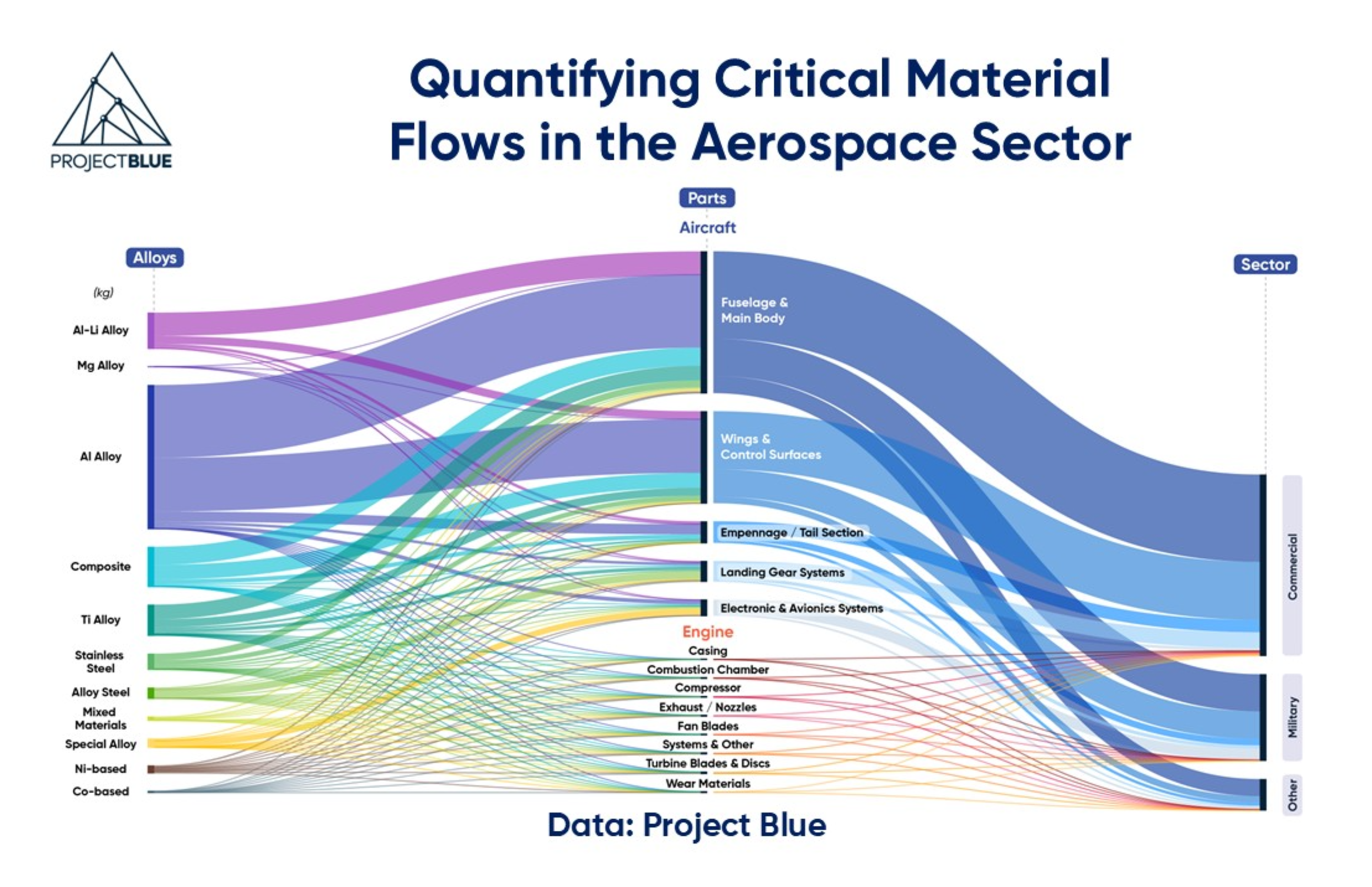
Quantifying critical material flows in the aerospace sector
Loading articles...